
i got a poker board, made by Fun World in the early 90's.

Roberto Fresca and i know this kind of boards already, as i dumped at least 2 of these boards in the last years. The big problem is, they are using a protection device (yellow chip on the board) and the program-code is decrypted.
if you remove the cover of this chip you get this (i broke two edges (3 pins) while removing the cover)

inside we have a (so far) unknown plcc28 chip and 3 DIE's...
Let's start with the DIE's from LEFT to RIGHT:
1.

a F245 from TI 1986...a octal latch
2.

can you see/identify the markings on the right top corner?

it's easier with a better microscope...had to order a better one.
it's a U65 from GTE
3.

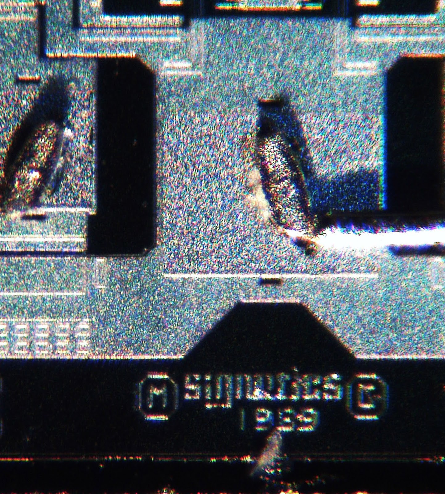
Need a better pic of the markings, but it's from SIGNETICS...
EDIT: better pics of the markings:

 does somebody know what this is?
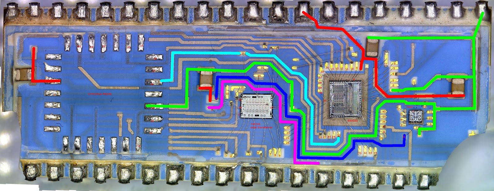
I'm pretty sure it's a 7400. It's got to be NAND or NOR because they are tying those inputs together to make an inverter, but the 7402 NOR has output on pin 1 and inputs on 2 and 3, so an unused NOR gate would have pin 1 not bonded and pins 2 and 3 grounded, which is not what we're seeing.
Pin 7 is the big pad at bottom center; the pins are numbered counterclockwise, so pin 1 is just right of top center. And the output is going to die 1, not the PROM.
It looks like die 1 is a TI 74F245A octal bus transceiver with tristate outputs. The output of the 7400 goes to pin 1, which is direction. Pins 10 and 20 are the giant pads on the top metal power layer; 10 on the right and 20 on the left.
and 30mins later:
Pin 1 is just *left( of top center and is an input along with pin 2, coming from a lower layer of the PCB. Pins 3, 4 and 5 are connected together, and pin 6 goes to the 74F245, pin 19, /OE.
another 30mins later:
I'm just confirming that things look correct; power and ground traces at first, then signals. It looks good so far; pin 30 of the 6502 is D3, and that's connected to pin 16 of the PROM, which is O3. That also goes to the 74F245 pin 15, so it can be gated out to one of the pins on the PCB.

EDIT: better pics of the markings:

Sean Riddle emailed me the following:
I think the 3rd die is a 74-series logic chip. You can see that there are 4 sections, each associated with 3 leads, plus power and ground. My guess is that it's address decoding for the PROM.
On the complete pic, you can see that the 2 sections on the right have the inputs grounded and the outputs aren't bonded. The top left section has 2 inputs coming from a middle layer, and the output is going to the 2 inputs of the bottom left section. The bottom left section's output goes to the PROM.
In your detail pic, it looks like there's text 00A, which might indicate 7400. Tying the inputs of the bottom left section together would make an inverter, meaning that the 2 inputs are being ANDed.
In your detail pic, it looks like there's text 00A, which might indicate 7400. Tying the inputs of the bottom left section together would make an inverter, meaning that the 2 inputs are being ANDed.
30mins later i got a second mail:
I'm pretty sure it's a 7400. It's got to be NAND or NOR because they are tying those inputs together to make an inverter, but the 7402 NOR has output on pin 1 and inputs on 2 and 3, so an unused NOR gate would have pin 1 not bonded and pins 2 and 3 grounded, which is not what we're seeing.
Pin 7 is the big pad at bottom center; the pins are numbered counterclockwise, so pin 1 is just right of top center. And the output is going to die 1, not the PROM.
It looks like die 1 is a TI 74F245A octal bus transceiver with tristate outputs. The output of the 7400 goes to pin 1, which is direction. Pins 10 and 20 are the giant pads on the top metal power layer; 10 on the right and 20 on the left.
and 30mins later:
Pin 1 is just *left( of top center and is an input along with pin 2, coming from a lower layer of the PCB. Pins 3, 4 and 5 are connected together, and pin 6 goes to the 74F245, pin 19, /OE.
another 30mins later:
I'm just confirming that things look correct; power and ground traces at first, then signals. It looks good so far; pin 30 of the 6502 is D3, and that's connected to pin 16 of the PROM, which is O3. That also goes to the 74F245 pin 15, so it can be gated out to one of the pins on the PCB.
4. and last the unknown PLCC28 chip (markings scratched off)

i/we think it could be a CY7C291A or CY7C168A, i need more time to try dumping it.
EDIT: I'm now 99% sure that it's a CY7C291A (thx to f205v, who gave this hint)
I already wired an adapter and dumped it.
As i bought a new microscope, i did highres pictures of the bit-area from the U65 chip (DIE #2) and stiched it together.
currently i don't know if it's a rom or ram area, but at least it's now documented and the 0's and 1's can be read by hand...
the goal is to understand the decryption of these poker boards. and i really hope it will be possible to dump the plcc28 chip.
if you want to support my work, the best way is to donate some money over paypal to crazy2001@cooltoad.com
all donated money will get used to buy new games or dumping equipment, like the new/better microscope.
No comments:
Post a Comment